Project Description

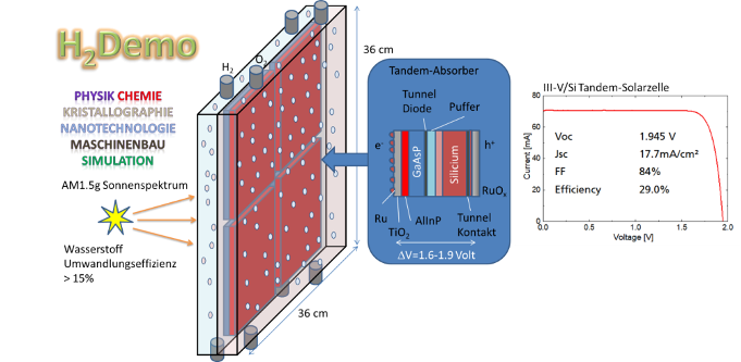
Figure: In the H2Demo project, a scalable demonstrator module for direct solar hydrogen production is being developed, which should achieve a conversion efficiency of at least 15% on an area of >36x36 cm2. The diagram shows the module concept on the left, the structure of the tandem absorber in the middle and the centre, and the characteristic curve of a III-V/Si tandem solar cell with optimal photovoltage for electrolysis. In the H2Demo project, these characteristics are to be achieved with a low-cost GaAsP/Si structure.
The aim of the H2Demo project is to produce the first large-scale demonstrators for direct solar hydrogen production. This is the absorption of sunlight in a semiconductor structure that generates a sufficiently large photovoltage > 1.6 volts to decompose water directly into hydrogen and oxygen. In the project, particularly promising tandem absorbers made of GaAsP/Si are being developed, which have the best chances of economic viability in combination with high efficiency and scalability. The III-V materials are characterised by very good stability and have already been investigated in detail in the BMBF-funded projects “III-V-Si” and “MehrSi”. By directly growing a few micrometre thin III-V layer on silicon, it was possible to produce solar cells that convert 25.9% of the energy of sunlight into electricity - this is an internationally observed world record for this technology [1, 2]. But there is still room for improvement, as the efficiency potential is even higher than 35%.
In the H2Demo project, the GaAsP/Si tandem absorbers are adapted to the requirements for hydrogen production, and growth conditions and the layer structure with its approximately 20 individual layers are optimised.
In addition, an H2 module concept is being developed on the basis of theoretical simulation calculations. The tandem absorbers are provided with protective layers that prevent corrosion, but at the same time have electronically passivating properties and enable charge exchange. Catalysts are applied to the protective layers, e.g. nanostructured rhodium or platinum. Using a similar approach and tandem GaInP/GaInAs absorbers, the project partners have already achieved the current efficiency record of 19% for direct photoelectrochemical water splitting in 2018.
Several measures are being taken to scale up and further improve the technology: More economical processes for the fabrication of GaAsP/Si tandem absorber layers will be developed, in particular by optimising growth rate, reactor throughput and gas utilisation in III-V epitaxy. New protective layers are applied to the absorbers by means of atomic layer deposition (ALD). These are thin layers of a few nm, some of which are already used in modern silicon solar cells. For the catalysts, new processes need to be developed for homogeneous deposition on large areas. This scaling up brings new challenges, but is a crucial step in demonstrating the relevance of direct water splitting.
At the end of the project, modules with a size of at least 1300 cm2 and a solar-to-hydrogen conversion efficiency > 15% are targeted. The materials and manufacturing processes are continuously reviewed for their scalability as well as environmental and economic aspects. The consortium of five companies (three of which are SMEs), four university groups and two non-university research institutions is taking on the task of demonstrating the benefits and potential of direct water splitting at the highest international level.
Check the links below for further information about the project: