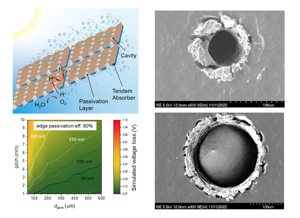
The H2Demo project aims to develop large-scale demonstrators for direct solar hydrogen production and one of the device concepts investigated is a porous photoelectrode design. The design allows for hydrogen and oxygen generation on the opposite sides of an integrated device, yet a direct pathway for mass transport is provided through the pores. At the same time, the edge of the pores could introduce recombination centers that are detrimental to the device performance. In order to determine the optimum design, H2Demo has developed a multiphysics model and simulated the voltage loss as a function of the design parameters (e.g., pore diameter, distance between pores). The parameter space that results in a minimum loss (< 100 mV) has been successfully identified and will be considered for the fabrication of the H2Demo demonstrators.
Our approach to experimentally realize the pores in tandem solar cell are laser-based drilling processes, which allow a fast processing of the high number of pores required. We are evaluating two different process sequences to realize pores in the tandem device:
(a) Laser drilling in the silicon bottom solar cell before III-V top cell growth and
(b) Laser drilling in the complete device after III-V top cell growth.
Currently, both process sequences are experimentally evaluated at Fraunhofer ISE, in order to identify the challenges related to both sequences and in the end, to identify the most promising and effective processing of porous tandem devices. Approach (a) comes, for instance, with the challenge to preserve the high-quality silicon surface required to grow the III-V cell on top. To address this, we are currently studying the III-V layer quality on such laser processed silicon bottom cell wafers (see SEM images). Approach (b), on the other hand, comes with the challenge to prevent electrical shunting in the laser-damaged regions at the side walls of the pores. For this approach, we are currently evaluating a promising processing sequence which allows to prevent the shunting effects, and therefore enables to compare the experimental results with the simulation model