
Atomic Layer Deposition of Protection Layers for III-V Photoelectrodes for Water Splitting
One of the main challenges in using III-V semiconductors in PEC setups is their poor stability in water. The use of optically transparent ‘window’ layers is widely considered to be the most promising protection strategy. TiO2 is a prime candidate for such window layers due to its optical transparency, good electron transport properties, and excellent chemical stability. In my PhD thesis work, I will focus on optimising TiO2 protection layers for various III-V tandem absorbers to achieve long-term stability under operation. The films will be deposited using atomic layer deposition (ALD). Using an in-line ALD-XPS-UPS system, where the XPS/UPS spectrum can be obtained after each sub-monolayer deposition, I observe how the nature and concentration of defects evolve during the growth of TiO2 films. Further, I study how nucleation of TiO2 occurs on the III-V surface and how different surface treatments influence the nucleation delay. For the TiO2 deposition, three different Ti precursors are considered (TDMAT, TTIP, TiCl4). Other parameters include substrate temperature, pulse and purge times, and the types of oxygen precursor (O2 plasma, H2O, O3). These studies will give insights on how different precursors react with the III-V surface.
The energetic alignment between these ALD interlayer, the underlying absorbers and the overlying catalyst will be optimized in order to minimize voltage losses in the system. The annealing of TiO2 films are performed under different atmosphere, time, and temperature, to observe how stability is influenced by crystallinity and morphology.
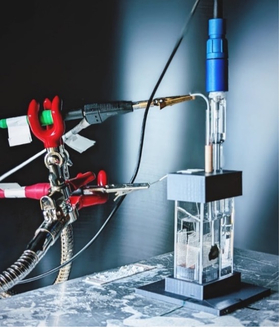
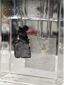
The stability is studied by photocurrent measurements as a function of time under different illumination conditions and pH values of the electrolyte. SEM and TEM are used to determine the nature of decay which occurs due to the gradual dissolution of TiO2 layer or the direct corrosion of the top absorber materials at the microscopic inhomogeneities in the layer, such as pinholes. The electronic passivation of protective layers is investigated by a combination of photoelectrochemical techniques. Linear Sweep Voltammetry (LSV) and OCP measurements will be used to determine the photocurrent and to gain insights on the photovoltage losses within the system. Intensity modulated photocurrent spectroscopy (IMPS) provides more detailed insights into the interplay between charge transfer and recombination processes at the semiconductor surfaces. Corrosion products are analysed with inductively coupled optical emission spectroscopy (ICP-OES).