
Analysis of crystalline defects and interfaces of III-V semiconductors grown on silicon by MOCVD for efficient and direct water splitting
In my PhD thesis I research to further improve the interface between the non-polar silicon (Si) substrate and the polar gallium phosphide (GaP) epitaxial buffer layer prepared in metalorganic vapour phase epitaxy (MOVPE) reactors. This involves control over the Si(100) surface preparation in atomic scale via optical spectroscopy prior to the GaP nucleation to avoid defects called antiphase domains in the GaP films. The obtained spectroscopic signals will be benchmarked with surface sensitive analytical tools in ultra-high vacuum. An additional challenge is to conduct this preparation at moderate temperatures with a short time, as annealing at elevated temperatures strongly limits the minority carrier lifetime. Other crystalline defects can be minimalized by an appropriate GaP nucleation step, which is free of three-dimensional islands and leads to a smooth GaP/Si heterointerface. The understanding of this heterointerface and suppression of recombination centres is crucial to achieve enough photovoltage for water splitting reaction and needs to be controlled on an atomic level. The developed processes will be transferred to the industrial MOVPE reactor at Fraunhofer ISE.
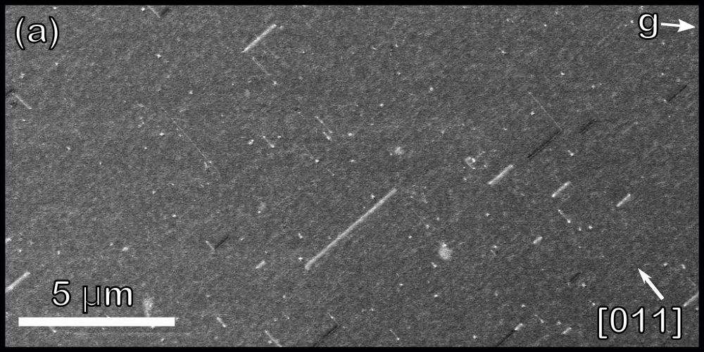
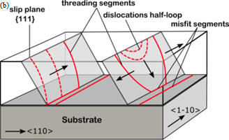
A very good tool to analyse defects in III-V buffers, such as stacking faults, stacking fault pyramids and misfit dislocations is electron channelling contrast imaging (ECCI). It is a non-destructive method which can image crystalline defects beneath the surface on a large scale. To understand the formation of the defects in dependence on the GaP nucleation procedure the partners from PUM will apply transmission electron microscopy to image the GaP/Si heterointerface in atomic scale.
Another aspect of research in the frame of this project is the interaction of the III-V/Si tandem photoabsorbers with the aqueous electrolyte. The stability and the photocorrosion processes need to be understood.