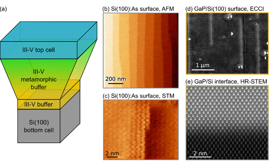
In the frame of this work package, either dual- or triple-junction III-V/Si absorber structures with a photovoltage above 1.7 V will be developed. To achieve this, photocurrent losses in the entire device need to be minimized. In particular, to be able to attain a higher photocurrent and a higher voltage, recombination centers at the GaP/Si heterointerface need to be identified and minimized, and defect densities in both the GaP nucleation layer and the III-V graded buffer layer need to be reduced below 105 cm-2 and 106 cm-2 respectively.
The growth parameters of GaAlP nucleation on Si(100) will be investigated, fine-tuned and transferred from the MOCVD reactor at TUIL to ISE. The defect density in the III-V buffer layers will be investigated by electron channeling contrast imaging (ECCI). A low-defect density in the GaP nucleation layer requires atomically well-ordered Si(100) surfaces, which need to be prepared in a short process and at the lowest possible temperature. In dependence on the Si(100) surface preparation, the electric field at the GaP/Si heterointerface will be modeled and investigated applying transmission electron microscopy (TEM) at PUM.
Variations of the structure, composition and growth parameters of the III-V step-graded metamorphic buffer between the GaP/Si and the subsequent photoabsorber will be conducted. The multi-junction photoabsorbers structures will be integrated with catalyst and anticorrosive layer in the WP3. Finally, the target structure will be grown with optimized bandgap energies of the sub-cells for maximum solar-to-hydrogen efficiency.
